Semiconductor Silicon Wafer Market
Surge in Demand for Consumer Electronics to Fuel Semiconductor Silicon Wafer Market Growth During Forecast Period
The demand for tablets, smartphones, wearables, and other consumer electronics devices, such as smartwatches, fitness trackers, VR headsets, and headsets, is increasing worldwide. These consumer electronics are used for various purposes, including accurate tracking of real-time data and providing enhanced convenience. According to the Groupe Speciale Mobile Association (GSMA), smartphone adoption across the globe was 76% in 2022, totaling 6.4 billion smartphone connections. The adoption is expected to reach 92% by 2030, making 9 billion connections worldwide. As per the same report, smartphone adoption in North America was 84% in 2022 and is expected to rise to 90% by 2030. Similarly, the smartphone adoption rate in Europe will boost from 84% in 2022 to 91% by 2030. In sub-Saharan Africa, an underpenetrated market, the smartphone adoption rate is predicted to grow from 51% in 2022 to 87% by 2030.
In multiple industries, wearables are utilized in tracking and managing personnel. For example, miners can be tracked under deep tunnels and alerted with a notification if signs of distress occur. Similarly, wearables are used for patients suffering from dementia to track their location if they go missing or get themselves in situations that require emergency help. As semiconductors such as silicon wafers can be used to manufacture chips and microchips in electronic devices, their demand is increasing worldwide. In addition, silicon wafers are used for the production of ICs, which is one of the important parts of various electronic devices, further boosting its demand. Thus, the growing demand for consumer electronics drives the semiconductor silicon wafer market.
Semiconductor Silicon Wafer Market: Industry Overview
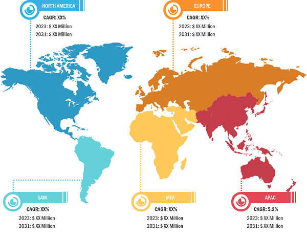
The semiconductor silicon wafer market is segmented on the basis of type, application, and node type. Based on type, the market is categorized into Upto 150 mm, diameter 200 mm, and diameter 300 mm and above. In terms of application, the market is segmented into consumer electronics, industrial, telecommunications, automotive, and others. Based on node type, the market is categorized into 180 nm, 130 nm, 90 nm, 65 nm, 45 nm, 22 nm, 14 nm, 7 nm, 5 nm and below, and others. By geography, the semiconductor silicon wafer market is segmented into North America, Asia Pacific, Europe, the Middle East & Africa, and South & Central America.
In terms of revenue, Asia Pacific dominated the semiconductor silicon wafer market share, followed by North America and Europe. Asia Pacific is the manufacturing hub for semiconductors. According to the Asian Development Bank, East and Southeast Asia account for over 80% of the world’s semiconductor output, which is critical for overall technological growth. This makes the world reliant on the region’s semiconductor exports, making its economic prospects also dependent on global semiconductor demand. Further, countries such as China are establishing government policies that benefit the semiconductor industry. This is expected to create considerable potential opportunities for the semiconductor silicon wafer market during the forecast period. The State Council of the People’s Republic of China, in April 2021, issued a framework that prioritizes the development of sophisticated semiconductor packaging solutions within the sector. Furthermore, according to material uploaded by a government-run agency, China is focusing on its aim to dominate advanced technologies of the future by establishing the world’s largest semiconductor state investment fund.
Governments of various countries across Asia Pacific are emphasizing on the development of the semiconductor industry. For example, the Government of India approved the building of three new semiconductor manufacturing facilities in February 2024 as part of the country’s flagship incentive program. In February 2024, the Union Cabinet approved three new semiconductor facilities as part of the “Development of Semiconductors and Display Manufacturing Ecosystems in India” agenda. The Prime Minister of India, Narendra Modi, virtually inaugurated these facilities on March 13, 2024. Similarly, from fiscal year 2021 to 2023, Japan has committed US$ 27 billion, or 0.71% of its GDP, in supplementary budgets to boost the semiconductor industry’s growth. Taiwan Semiconductor Manufacturing Company, the world’s largest chipmaker, received US$ 8.4 billion in funding to build a plant in Kikuyo, Kumamoto Prefecture. Similarly, Rapidus, a Japanese chipmaker, received US$ 6.45 billion to develop next-generation semiconductor technology.
Semiconductor Silicon Wafer Market: Competitive Landscape and Key Developments
Okmetic; Wafer Works Corp; SUMCO CORPORATION; NANOCHEMAZONE; Alfa Chemistry; LONGi Green Energy Technology Co Ltd; Wafer World Inc.; WaferPro; PI-KEM Limited; Nano Quarz Wafer GmbH; Sino-American Silicon Products Inc.; Nanografi Nano Technology; Fujimi Incorporated; Hangzhou Semiconductor Wafer Co., Ltd.; Ferrotec Holdings Corporation; Silicon Materials, Inc.; Shin-Etsu Chemical Co Ltd; SK Siltron Co., Ltd.; Siltronic AG; and GlobalWafers Co., Ltd. are among the leading players profiled in the semiconductor silicon wafer market report. Several other essential market players were analyzed for a holistic view of the market and its ecosystem. The semiconductor silicon wafer market report provides detailed market insights, which help the key players strategize their market growth. As per the company press releases, a few key developments are mentioned below:
- LONGi Green Energy Technology Co., Ltd. officially announced the new world record efficiency of 30.1% for the commercial M6 size wafer-level silicon-perovskite tandem solar cell at the 2024 Intersolar Europe in Munich, Germany.
(Source: LONGi Green Energy Technology Co., Ltd., Press Release, June 2024)
- Okmetic—the supplier of advanced silicon wafers used for manufacturing MEMS, sensors, RF, and power devices—has announced the release of an Engineered Ultra High Resistivity wafer, a premium silicon substrate dedicated to demanding RF filters and devices. This highly advanced wafer technology leverages Okmetic’s proprietary A-MCzÒ crystal growth process to deliver the highest resistivity and best technical performance in the form of approximately zero substrate-induced losses and nonlinearities for RF devices. Also, Okmetic Ultra High Resistivity wafers’ oxygen content is optimized, which improves wafer strength and makes them a viable option for ultra-high resistivity FZ wafers.
(Source: Okmetic, e, Press Release, March 2021)